The forum is currently inactive due to too much AI spam.
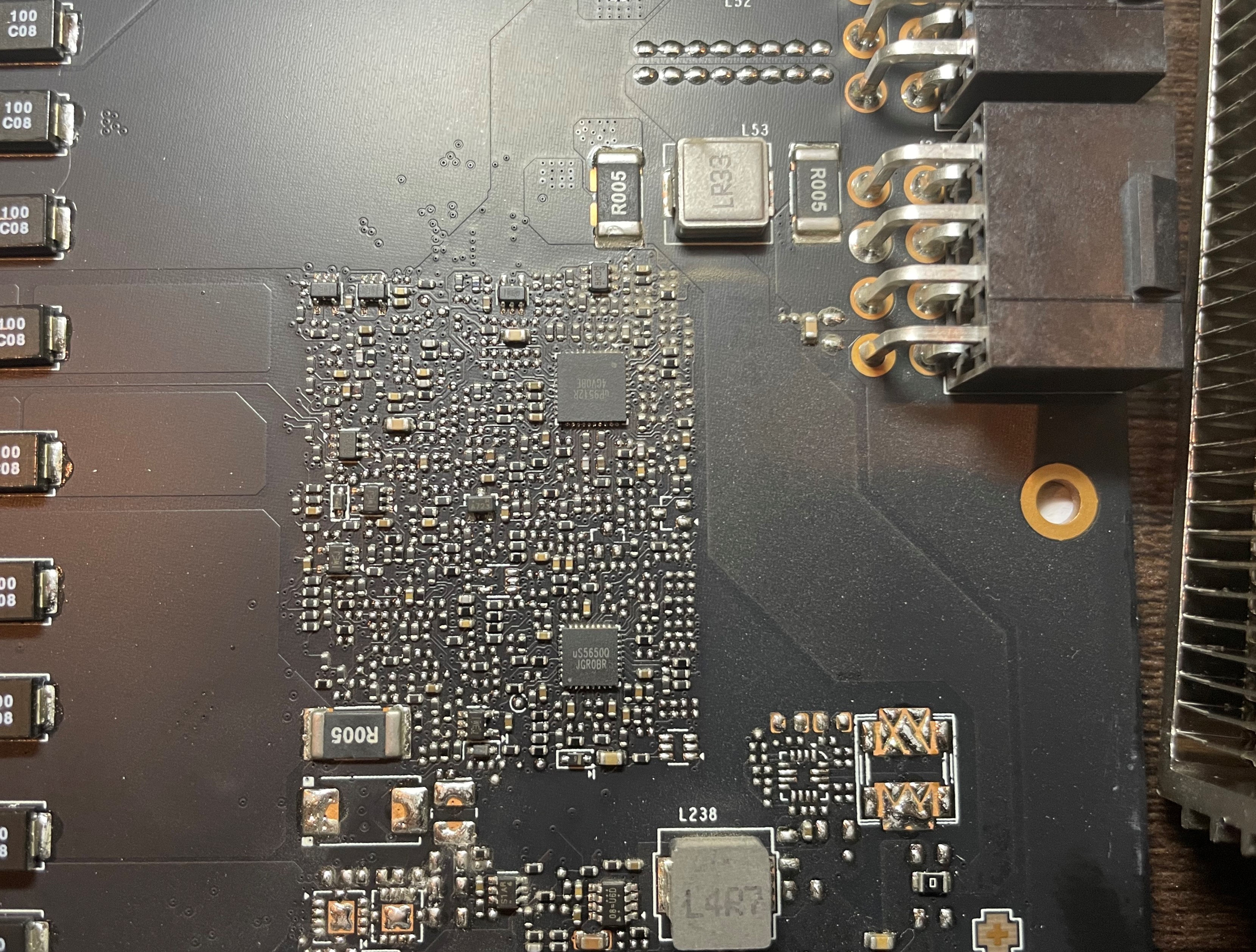
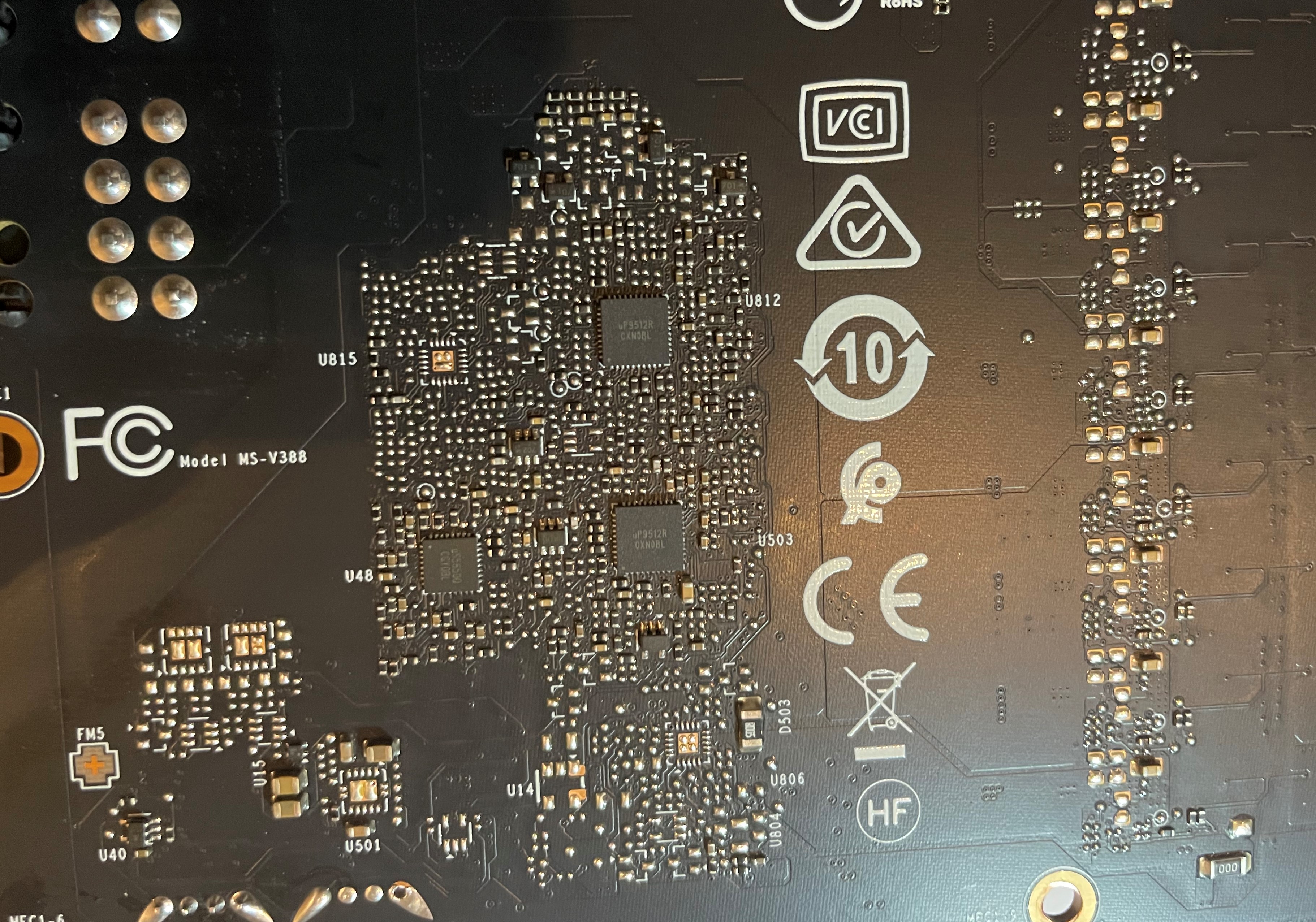
MSI GeForce RTX 3090 AERO attach point, EVC2SX,uP9512R
Quote from Bruce on 2021-05-01, 22:25Hello there,
I was wondering if someone could help me with my MSI GeForce RTX 3090 AERO.
Is there any i2c attach points for my EVC2SX ?
Voltage controller: uP9512R
Thanks!
Hello there,
I was wondering if someone could help me with my MSI GeForce RTX 3090 AERO.
Is there any i2c attach points for my EVC2SX ?
Voltage controller: uP9512R
Thanks!
Uploaded files: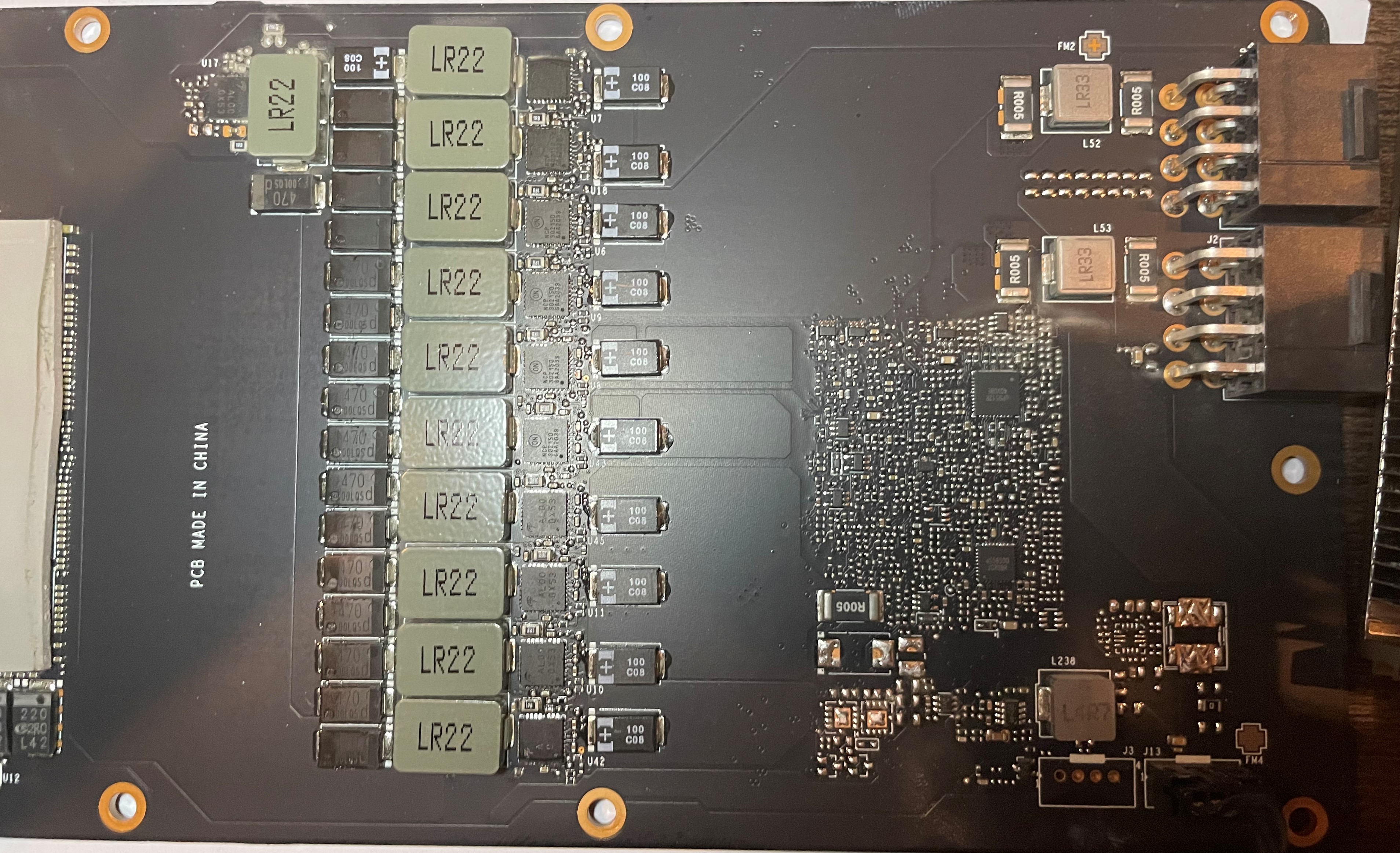
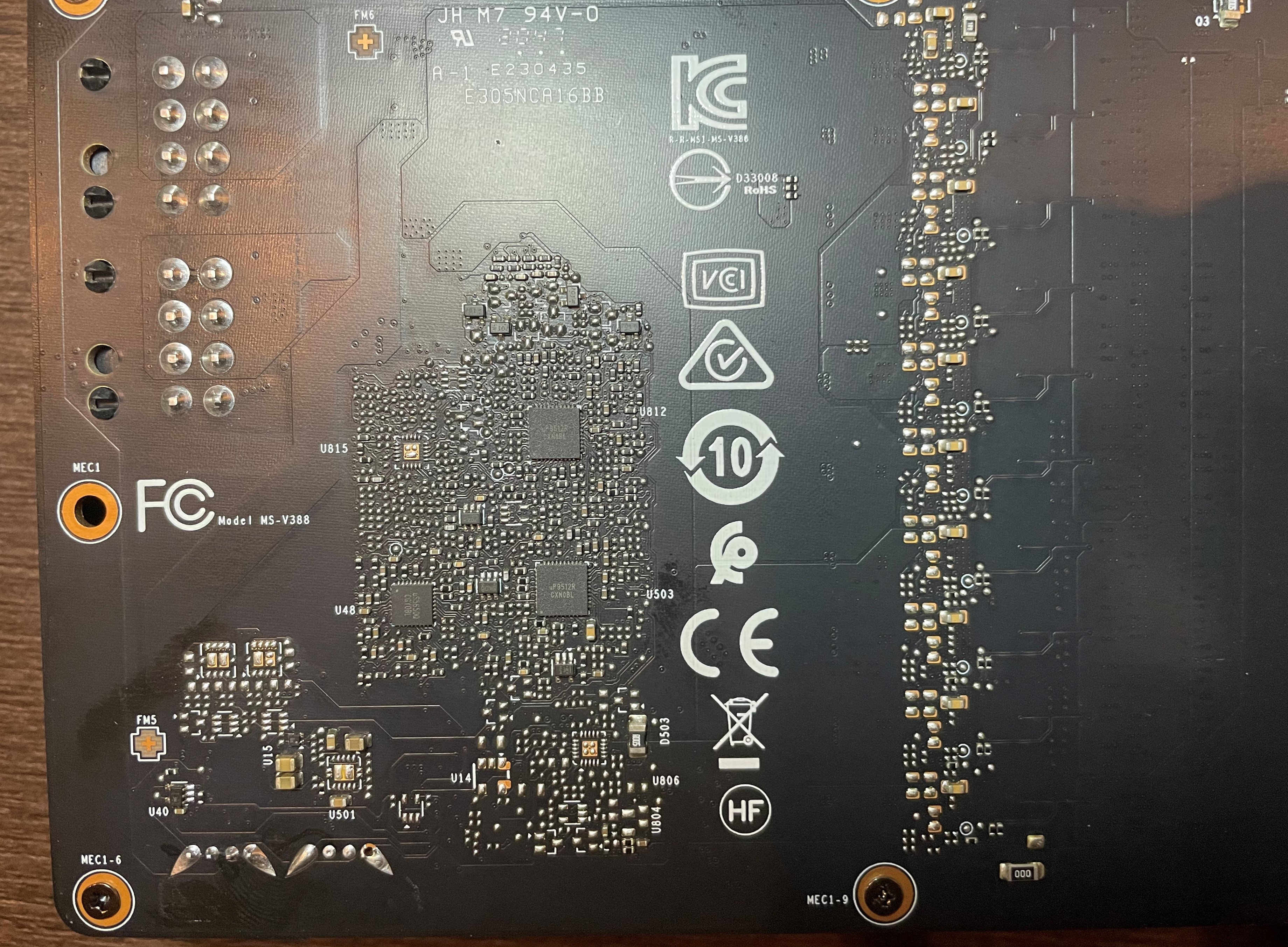
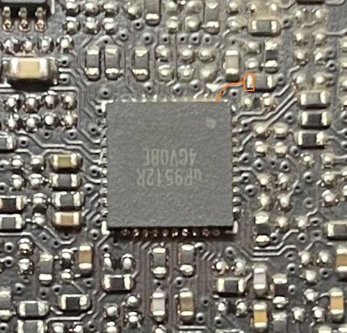
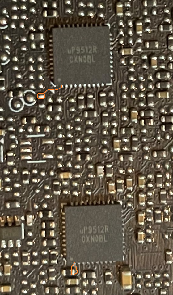
Quote from elmor on 2021-05-02, 08:01Hello, I tried to trace the pins from the controllers based on your picture. See the attached image.
Hello, I tried to trace the pins from the controllers based on your picture. See the attached image.
Uploaded files:
Quote from Bruce on 2021-05-02, 17:08Quote from elmor on 2021-05-02, 08:01Hello, I tried to trace the pins from the controllers based on your picture. See the attached image.
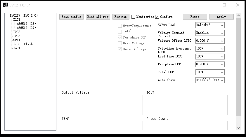
Thanks for your reply. It works. My EVC2SX has successfully connected to the uP9512R.
I want to control the GPU voltage. But there is no controller like MP2888A can be found on i2c bus. Any suggestions?
Quote from elmor on 2021-05-02, 08:01Hello, I tried to trace the pins from the controllers based on your picture. See the attached image.
Thanks for your reply. It works. My EVC2SX has successfully connected to the uP9512R.
I want to control the GPU voltage. But there is no controller like MP2888A can be found on i2c bus. Any suggestions?
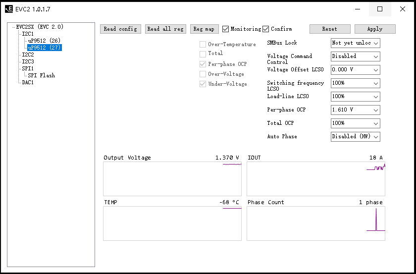
Quote from elmor on 2021-05-03, 09:04I didn't see any MP2888A controller on that card, so I don't see why you would expect to find one. There seems to be 3x uP9512 so I'm not sure why you're only finding 2x and not 3x of them. One should be for GPU voltage, another for MSVDD and the third one for memory voltage. What is the voltage reading from the uP9512 at address 26 and address 27?
I didn't see any MP2888A controller on that card, so I don't see why you would expect to find one. There seems to be 3x uP9512 so I'm not sure why you're only finding 2x and not 3x of them. One should be for GPU voltage, another for MSVDD and the third one for memory voltage. What is the voltage reading from the uP9512 at address 26 and address 27?
Quote from Bruce on 2021-05-03, 10:46Quote from elmor on 2021-05-03, 09:04I didn't see any MP2888A controller on that card, so I don't see why you would expect to find one. There seems to be 3x uP9512 so I'm not sure why you're only finding 2x and not 3x of them. One should be for GPU voltage, another for MSVDD and the third one for memory voltage. What is the voltage reading from the uP9512 at address 26 and address 27?
I thought uP9512 was for memory voltage control only.
0.75V at 26 and 1.37V at 27. The third one is on the other side of the PCB. Is there any other i2c bus? Shall I solder to it?
The voltage offset of uP9512 is limited to 0 ~ 150mV. Can I reduce the GPU voltage in this way?
Quote from elmor on 2021-05-03, 09:04I didn't see any MP2888A controller on that card, so I don't see why you would expect to find one. There seems to be 3x uP9512 so I'm not sure why you're only finding 2x and not 3x of them. One should be for GPU voltage, another for MSVDD and the third one for memory voltage. What is the voltage reading from the uP9512 at address 26 and address 27?
I thought uP9512 was for memory voltage control only.
0.75V at 26 and 1.37V at 27. The third one is on the other side of the PCB. Is there any other i2c bus? Shall I solder to it?
The voltage offset of uP9512 is limited to 0 ~ 150mV. Can I reduce the GPU voltage in this way?
Uploaded files: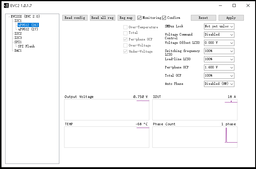
Quote from elmor on 2021-05-04, 09:17Quote from Bruce on 2021-05-03, 10:46Quote from elmor on 2021-05-03, 09:04I didn't see any MP2888A controller on that card, so I don't see why you would expect to find one. There seems to be 3x uP9512 so I'm not sure why you're only finding 2x and not 3x of them. One should be for GPU voltage, another for MSVDD and the third one for memory voltage. What is the voltage reading from the uP9512 at address 26 and address 27?
I thought uP9512 was for memory voltage control only.
0.75V at 26 and 1.37V at 27. The third one is on the other side of the PCB. Is there any other i2c bus? Shall I solder to it?
The voltage offset of uP9512 is limited to 0 ~ 150mV. Can I reduce the GPU voltage in this way?
On that card it seems separate uP9512 is used for all rails. It could be that the other uP9512 is on another I2C bus, but I haven't seen any case like that so far. The SDA trace is also tricky on the other side because it goes straight into a via. You could check with a multimeter if the SDA/SCL pins are connected to the other side.
Sorry the uP9512 only offers limited voltage adjustment between 0 to +150mV.
Quote from Bruce on 2021-05-03, 10:46Quote from elmor on 2021-05-03, 09:04I didn't see any MP2888A controller on that card, so I don't see why you would expect to find one. There seems to be 3x uP9512 so I'm not sure why you're only finding 2x and not 3x of them. One should be for GPU voltage, another for MSVDD and the third one for memory voltage. What is the voltage reading from the uP9512 at address 26 and address 27?
I thought uP9512 was for memory voltage control only.
0.75V at 26 and 1.37V at 27. The third one is on the other side of the PCB. Is there any other i2c bus? Shall I solder to it?
The voltage offset of uP9512 is limited to 0 ~ 150mV. Can I reduce the GPU voltage in this way?
On that card it seems separate uP9512 is used for all rails. It could be that the other uP9512 is on another I2C bus, but I haven't seen any case like that so far. The SDA trace is also tricky on the other side because it goes straight into a via. You could check with a multimeter if the SDA/SCL pins are connected to the other side.
Sorry the uP9512 only offers limited voltage adjustment between 0 to +150mV.
Uploaded files: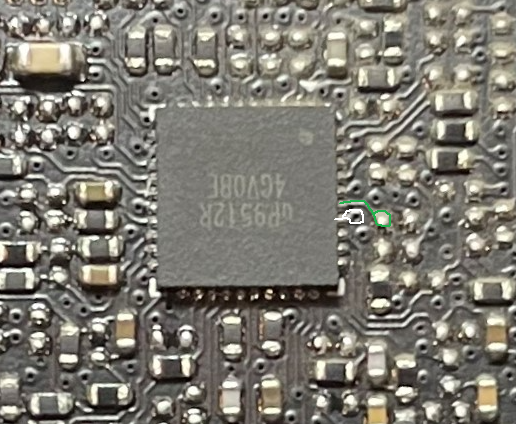
Quote from Bruce on 2021-05-04, 21:24Quote from elmor on 2021-05-04, 09:17Quote from Bruce on 2021-05-03, 10:46Quote from elmor on 2021-05-03, 09:04I didn't see any MP2888A controller on that card, so I don't see why you would expect to find one. There seems to be 3x uP9512 so I'm not sure why you're only finding 2x and not 3x of them. One should be for GPU voltage, another for MSVDD and the third one for memory voltage. What is the voltage reading from the uP9512 at address 26 and address 27?
I thought uP9512 was for memory voltage control only.
0.75V at 26 and 1.37V at 27. The third one is on the other side of the PCB. Is there any other i2c bus? Shall I solder to it?
The voltage offset of uP9512 is limited to 0 ~ 150mV. Can I reduce the GPU voltage in this way?
On that card it seems separate uP9512 is used for all rails. It could be that the other uP9512 is on another I2C bus, but I haven't seen any case like that so far. The SDA trace is also tricky on the other side because it goes straight into a via. You could check with a multimeter if the SDA/SCL pins are connected to the other side.
Sorry the uP9512 only offers limited voltage adjustment between 0 to +150mV.
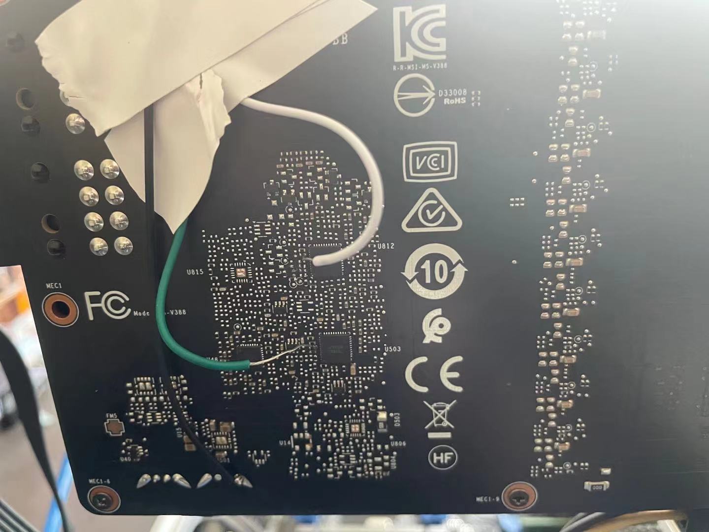
OK, a little disappointed with this card. After reading the VMOD-header Tutorial, I am trying to use the VMOD header to reduce the GPU voltage.
But I don't know where is FB and Vout pin or pins on this PCB. Can you help to figure it out, please.
Quote from elmor on 2021-05-04, 09:17Quote from Bruce on 2021-05-03, 10:46Quote from elmor on 2021-05-03, 09:04I didn't see any MP2888A controller on that card, so I don't see why you would expect to find one. There seems to be 3x uP9512 so I'm not sure why you're only finding 2x and not 3x of them. One should be for GPU voltage, another for MSVDD and the third one for memory voltage. What is the voltage reading from the uP9512 at address 26 and address 27?
I thought uP9512 was for memory voltage control only.
0.75V at 26 and 1.37V at 27. The third one is on the other side of the PCB. Is there any other i2c bus? Shall I solder to it?
The voltage offset of uP9512 is limited to 0 ~ 150mV. Can I reduce the GPU voltage in this way?
On that card it seems separate uP9512 is used for all rails. It could be that the other uP9512 is on another I2C bus, but I haven't seen any case like that so far. The SDA trace is also tricky on the other side because it goes straight into a via. You could check with a multimeter if the SDA/SCL pins are connected to the other side.
Sorry the uP9512 only offers limited voltage adjustment between 0 to +150mV.
OK, a little disappointed with this card. After reading the VMOD-header Tutorial, I am trying to use the VMOD header to reduce the GPU voltage.
But I don't know where is FB and Vout pin or pins on this PCB. Can you help to figure it out, please.

Quote from elmor on 2021-05-09, 12:39I'm not sure which controller is for which output, but for uP9512 the best would be to modify the REFIN pin just like this video. The procedure is the same on uP9511 and uP9512. https://www.youtube.com/watch?v=X3Y_zbJOb7E
I'm not 100% the routing I found is correct so I suggest you try to check if pin #1 (REFIN) is really connected to these points.
I'm not sure which controller is for which output, but for uP9512 the best would be to modify the REFIN pin just like this video. The procedure is the same on uP9511 and uP9512. https://www.youtube.com/watch?v=X3Y_zbJOb7E
I'm not 100% the routing I found is correct so I suggest you try to check if pin #1 (REFIN) is really connected to these points.
Uploaded files: